Assembly & Test
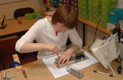

The small batch sizes associated with our business result in most electronic assembly and test being performed manually. All components and pcb finishes are now lead-free, although tin/lead solders are still employed on some RoHS exempt work. Great care is taken to segregate the two types of soldering operation. The need for good ground planes in microwave and RF work gives rise to a high degree of heat sinking during soldering, making it frequently necessary to employ background heat, particularly in the lead free-case.
Anti-static precautions are taken in all stages of electronic assembly, and we consider it good design practice to include high-valued resistors to ground on all pcb input and output lines.
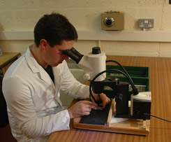
All assembled pcb's are fully inspected under the microscope before being installed in housings and powered up. We have found that virtually all potential faults due to assembly problems can be identified and rectified at this stage. Following final assembly and test, all sub-units are visually inspected once more before the units are sealed.
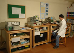
All production test gear is maintained in good order and kept in calibration. As with R & D instrumentation, we only buy new or refurbished items directly from the manufacturer, and use the manufacturers' calibration facilities wherever possible for all microwave and RF instruments.
In many production contracts, particularly for more complex sources and sub-systems, considerable effort is put into building special test gear for both sub-unit and final test to ensure production proceeds as smoothly and quickly as possible.
Following test, all sub-units and final assemblies are inspected, sealed and labelled, the label carrying the signatures of the persons responsible for test and inspection.
Production test gear requiring RF modules can often be assembled quickly using our "Curikela" range of RF constructional kits.